The 2-nanometer trap: Why Germany's chip strategy is insufficient for the future
Xpert Pre-Release

Available in 27 languages 📢
Prefer Xpert.Digital on GoogleⓘPublished on: August 22, 2026 / Updated on: August 22, 2026 – Author: Konrad Wolfenstein
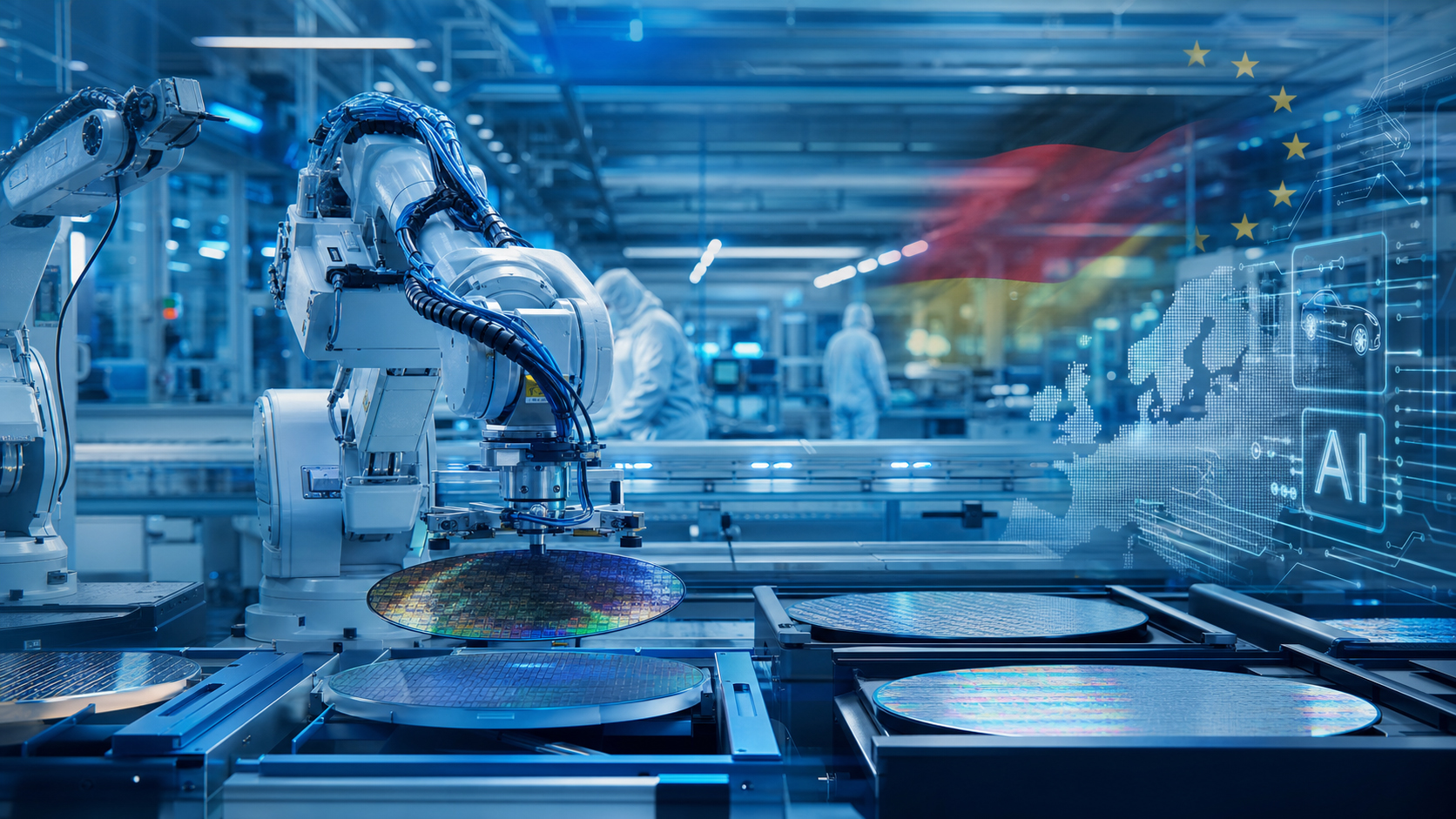
The 2-nanometer trap: Why Germany's chip strategy is insufficient for the future – Image: Xpert.Digital
A warning to industry: Without these super chips, Germany will become nothing more than a mere assembly plant
Billions spent on outdated technology? Why "Silicon Saxony" won't save us from AI collapse
From car manufacturer to supplier: The bleak scenario for the German economy
German industry stands at a historic turning point: Decades of economic success, primarily driven by mechanical engineering, precision mechanics, and the internal combustion engine, are rapidly losing momentum in the age of artificial intelligence and cloud computing. While politicians celebrate billions in subsidies and the establishment of new chip factories in so-called "Silicon Saxony," these merely serve the mature technology hubs of today. The true revolution—the foundation for autonomous driving, embodied robotics, and future systems dominance—is taking place in the extremely miniaturized realm of 2-nanometer semiconductors. So far, Europe is at best a research hub in this crucial cutting-edge field, while commercial mass production is dominated by Asian and American players. If Germany fails to quickly establish its own gigafactories for these super-chips, the once-exporting nation faces a fatal fate: degradation to a mere assembly line for the software giants of other continents. The following article analyzes the harsh physical, economic, and geopolitical realities that will determine Germany's industrial survival.
Race for future viability: Why the semiconductor question will determine Germany's industrial existence
Germany needs its own production base for 2-nanometer chips; otherwise, the country will rapidly lose its international competitiveness in the next fifteen years. This thesis may sound alarmist at first, but it is based on a sober analysis of the physical, economic, and geopolitical realities that currently shape the global semiconductor industry. Anyone who reduces the debate about Germany as a chip manufacturing location to the Dresden cluster overlooks the tectonic shifts taking place in the value chain of future technologies.
Between Silicon Saxony and world leaders: Where Germany really stands today
In public debates about Germany as a semiconductor location, the Dresden cluster, known as Silicon Saxony, is regularly cited. There, established manufacturing processes from 28 nanometers upwards currently dominate, which are perfectly adequate and extremely reliable for classic industrial controls, sensors, power electronics, and chassis control systems. The joint project of TSMC, Bosch, Infineon, and NXP, called the European Semiconductor Manufacturing Company, began construction in Dresden in August 2024 with a symbolic groundbreaking ceremony. With a total investment of more than ten billion euros, the project aims to produce around 40,000 wafers per month in the 300-millimeter format.
The facility focuses on the 28 and 22 nanometer technology nodes using planar CMOS technology, as well as the 16 and 12 nanometer FinFET technology, and is primarily aimed at the European automotive and industrial electronics sectors. The German government is funding the project with up to five billion euros, which corresponds to approximately half of the total investment. Construction is currently in the cleanroom installation phase, with production scheduled to begin in 2027. This factory is an important and long-overdue step towards European chip sovereignty, but it deliberately does not target the cutting edge of manufacturing.
However, anyone who believes that German industry can survive in the long term with manufacturing nodes in the 28 nanometer range alone fundamentally misunderstands the rules of the game for the coming decade.
The computing hunger of the future: Why 2-nanometer chips are the new industrial backbone
The 2-nanometer tip node is no longer just a tool for miniaturizing smartphones or laptops. It forms the physical foundation for cloud computing, artificial intelligence, robotics in the sense of embodied AI, and autonomous driving. If Germany wants to maintain a leading role in the global automotive industry, robotics, and advanced manufacturing, a domestic value chain for this cutting-edge technology is not a dispensable luxury, but a long overdue strategic necessity.
The European Chips Act explicitly states this goal, aiming to increase the European Union's global market share in state-of-the-art semiconductors from its current level of around ten percent to at least twenty percent by 2030, expressly including the production of chips at 2 nanometers and below. To illustrate the scale: one nanometer is one billionth of a meter, while a human hair measures approximately 80,000 to 100,000 nanometers. Two nanometers is roughly the thickness of a DNA strand, highlighting the sheer physical dimension of this technology.
Why autonomous driving is reaching its physical performance limits
Autonomous driving illustrates the underlying dilemma in a particularly vivid way. During the transition from partially automated systems of Level 2 Plus to fully autonomous systems of Levels 4 and 5, in-vehicle supercomputers must process the data from dozens of high-resolution sensors in real time while simultaneously executing billions of parameters in artificial intelligence's vision and action models. The computing power required increases from a few hundred to several thousand TOPS, or trillions of operations per second.
In practical terms, this exponentially increasing demand leads directly to the so-called power wall. Energy efficiency, measured in TOPS per watt, becomes a matter of survival for the entire vehicle architecture. Older manufacturing nodes would consume several hundred watts, up to a kilowatt, of electrical power for a computing requirement of several thousand TOPS. This not only drastically reduces the battery range of an electric vehicle but also necessitates heavy and expensive liquid cooling systems within the vehicle itself. The efficiency gains offered by a 2-nanometer process compared to older nodes therefore directly determine whether AI systems remain economically scalable in production vehicles.
Furthermore, there is the safety relevance in the area of latency. At a speed of 130 kilometers per hour, every millisecond of processing delay translates to several meters of additional braking distance. Only the enormous transistor density made possible by a 2-nanometer process allows for the integration of huge neural processing units and high-bandwidth memory onto a single system-on-chip, thereby reducing processing latencies to a technically acceptable minimum.
From machine manufacturer to supplier of third-party system architectures
Germany undoubtedly boasts world-class engineering expertise at companies like BMW, Mercedes-Benz, Volkswagen, and KUKA. However, in the age of what is sometimes referred to as Industry 5.0, industrial value creation is rapidly shifting from mechanics and chassis technology to semantics, computing power, and algorithms. Without its own, or at least reliably secured, manufacturing and design infrastructure for cutting-edge chip technology, German industry faces a triple structural risk.
The first risk lies in the vulnerability of supply chains. In this scenario, high-end processors remain permanently dependent on overseas contract manufacturers, and geopolitical upheavals could cripple key industries overnight. The second risk is the loss of system sovereignty. Companies that cannot co-design chips from the ground up must resort to standard solutions and thus lose the ability to achieve deep integration between hardware and software, which is crucial, especially in safety-critical applications like autonomous driving. The third risk is the reduction to mere hardware assembly. The scenario looms of building mechanically excellent but technologically dependent shells for the software giants of other continents.
This development would be of existential importance for a country whose economic prosperity has been based for decades on the export of high-quality industrial goods. The automotive industry alone represents one of Germany's largest economic sectors, and its focus of value creation is increasingly shifting from mechanical manufacturing to software and chip architecture.
Our EU and German expertise in business development, sales and marketing

Our EU and German expertise in business development, sales and marketing - Image: Xpert.Digital
Industry focus areas: B2B, digitalization (from AI to XR), mechanical engineering, logistics, renewable energies and industry
More information here:
A thematic hub offering insights and expertise:
- Knowledge platform covering global and regional economies, innovation and industry-specific trends
- A collection of analyses, insights, and background information from our key areas of focus
- A place for expertise and information on current developments in business and technology
- A hub for companies seeking information on markets, digitalization, and industry innovations
Europe's path to 2-nanometer chip manufacturing: Opportunities and obstacles for Germany
The European toolbox: ASML, Imec and the Chip Act pilot lines
TSMC's initial focus on manufacturing nodes in the 28 to 12 nanometer range with its joint venture with ESMC in Dresden is an important first step towards building a complete industrial ecosystem encompassing chemicals, ultrapure water, skilled workers, and packaging technology. However, this should only be the springboard for the next, significantly more ambitious step.
With the tools of the European Chips Act, the locational advantages of the Dutch lithography world market leader ASML in neighboring Holland, and the research strength of the Belgian research institute Imec, Europe already possesses essential building blocks for establishing its own cutting-edge manufacturing capabilities. In the summer of 2026, the European Union commissioned a €2.5 billion investment in the so-called NanoIC pilot line at the Imec site in Leuven, the first European facility to utilize the most advanced extreme ultraviolet lithography systems, which are essential for the production of 2-nanometer chips and below. Simultaneously, the FAMES pilot line, focusing on energy-efficient FD-SOI technology, began operation in January 2026 at the French research center CEA-Leti in Grenoble.
Under the umbrella of the Chips Act, five pilot lines are planned, representing a combined investment of €3.7 billion from EU funds and national contributions, while the total politically initiated investment is projected to exceed €100 billion by 2030. However, these pilot lines are primarily focused on research, prototype development, and testing at a near-industrial scale and do not yet constitute commercial mass production. The crucial next step that Europe must now force is the actual establishment of fully-fledged 2-nanometer-class gigafactories on its own soil, transitioning from the research phase to profitable mass production.
Capital intensity as a bottleneck: The economic reality of a 2nm factory
The economic dimension of a state-of-the-art manufacturing facility should not be underestimated. While the ESMC factory in Dresden for mature process nodes already requires more than ten billion euros in investment, the costs for a fully-fledged 2-nanometer-class factory are significantly higher, as the necessary extreme ultraviolet lithography systems, highly specialized cleanrooms, and extremely complex process steps require several times the investment sum for mature nodes. In addition, there are structural location disadvantages that put the European, and especially the German, semiconductor sector at a disadvantage compared to competing regions such as Taiwan, South Korea, or the United States.
The comparatively high energy prices in Germany represent a significant cost factor for energy-intensive chip manufacturing, as modern factories for cutting-edge nodes require enormous amounts of electricity for lithography systems, cleanroom climate control, and process cooling. At the same time, constructing such a facility requires a substantial capital investment, which only pays for itself with sufficient capacity utilization and stable demand over many years. The shortage of skilled workers in highly specialized areas of semiconductor physics and process engineering further exacerbates the challenge, as training such experts takes years and is a scarce resource in the international competition for talent.
Between ambition and realism: Is 2nm manufacturing even achievable in Germany?
Given these circumstances, the question rightly arises whether Germany can actually establish a functioning factory for 2-nanometer chips within the next ten years, despite high energy prices and considerable investment pressure. Developments to date present a mixed picture. On the one hand, the German government has demonstrated its willingness to provide billions in subsidies for the development of a domestic semiconductor industry by supporting the ESMC factory in Dresden, and the European pilot lines in Belgium and France show that the necessary research infrastructure for cutting-edge technology can indeed be developed in Europe.
On the other hand, the commercial mass production of 2-nanometer chips remains the domain of a few suppliers outside Europe, whose technological lead has been built on decades of investment and tightly integrated supply chains. A realistic path for Germany and Europe is therefore unlikely to lie in going it alone entirely, but rather in a strategic combination of strengthened domestic research capacities, targeted partnerships with leading contract manufacturers, and a consistent political prioritization of the necessary framework conditions regarding energy costs, approval processes, and skilled worker training.
From the combustion engine to silicon: The shift in the industrial power base
The foundation of German industry in the last century was precision mechanics, the internal combustion engine, and control chips at 28 nanometers. The backbone of the next thirty years, however, will be highly efficient supercomputing power made from 2-nanometer silicon. This shift marks a fundamental break with Germany's previous industrial success model, which for generations was based on mechanical precision, materials science, and systems integration.
The crucial question for the coming years is therefore not whether Germany can be content with mature manufacturing hubs, but rather how quickly and consistently the country can create the necessary investments, political frameworks, and industrial partnerships to avoid remaining permanently dependent on other continents for cutting-edge semiconductor manufacturing technology. The ongoing European initiatives in Dresden, Leuven, and Grenoble demonstrate the will to establish a domestic semiconductor base, but the path from research pilot line to profitable 2-nanometer-class gigafactory remains the true litmus test for Germany's and Europe's technological sovereignty in the decades to come.
🎯🎯🎯 Data-driven B2B industry hub as a quasi-in-house solution

The quasi-in-house solution: How Xpert.Digital closes operational gaps in B2B marketing and sales – Smart Content-Driven Business - Image: Xpert.Digital
Xpert.Digital is a data-driven B2B industry hub led by Konrad Wolfenstein . The company acts as an external, quasi-in-house solution for industrial partners, closing operational gaps in marketing, content, and sales – without requiring additional resources on the client side.
More information here:
Your global marketing and business development partner
☑️ Our business language is English or German
☑️ NEW: Correspondence in your native language!

Konrad Wolfenstein
I and my team are happy to be available to you as your personal advisor.
You can contact me by filling out the contact form here [email protected]:or simply call me at +49 7348 4088 965. My email address is
I'm looking forward to our joint project.