Germany's secret chip monopoly: Why the tech world depends on Swabia and Hesse
Xpert Pre-Release

Available in 27 languages 📢
Prefer Xpert.Digital on GoogleⓘPublished on: August 4, 2026 / Updated on: August 4, 2026 – Author: Konrad Wolfenstein
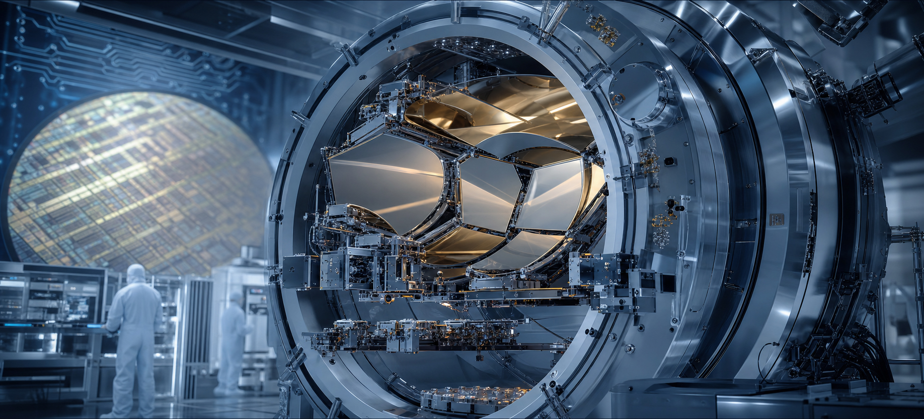
Germany's secret chip monopoly: Why the tech world depends on Swabia and Hesse – Image: Xpert.Digital
Without this German component, global semiconductor production comes to a standstill – the hardware behind ChatGPT and Co.
No AI revolution without German technology: The DNA of the most modern microchips
When politicians and economic strategists debate technological sovereignty, artificial intelligence, and the future of the semiconductor industry, their focus is usually on Taiwan, Silicon Valley, or the highly subsidized new megafactories in Dresden and Magdeburg. But this fixation on chip manufacturing locations overlooks the real, critical bottleneck of the entire industry: two unassuming small towns in Baden-Württemberg and Hesse. In Oberkochen and Wetzlar, Carl Zeiss SMT GmbH develops and produces the extremely complex mirror optics without which the Dutch industry leader ASML cannot build modern lithography systems. Conversely, this means that without precision optics from Swabia and Hesse, there would be no highly integrated microchips worldwide for smartphones, data centers, or AI accelerators. The following analysis sheds light on how this unprecedented, natural double monopoly arose over decades, why it gives Germany an unforeseen geopolitical power position, and why the construction of ever new chip factories worldwide does not reduce the dependence on these two German locations, but rather drastically exacerbates it.
The 350-million-euro bottleneck: Why Germany controls the chip market
The bottleneck of the global economy: Why every chip factory depends on these two small German towns
When politicians and industry strategists discuss technological sovereignty in semiconductor manufacturing, their attention almost reflexively turns to Taiwan, the new factories in Arizona, or the multi-billion-euro funding programs in Dresden and Magdeburg. What is regularly overlooked is that the real technological bottleneck for the entire industry lies in two comparatively inconspicuous locations in Germany: Oberkochen in Baden-Württemberg and Wetzlar in Hesse. There, Carl Zeiss SMT GmbH, the semiconductor division of the Zeiss Group, develops and manufactures the projection optics for the lithography systems of the Dutch machine manufacturer ASML. Without these optics, no modern EUV system can be built, and without an EUV system, no highly integrated chips in the single-digit nanometer range can be produced, as needed for smartphones, data centers, and especially for the accelerator chips of artificial intelligence. According to Zeiss SMT, around 80 percent of all microchips manufactured worldwide contain lithography optics of German origin; for the most sophisticated chips used in AI applications, the figure is practically 100 percent. This analysis examines how this dependency arose, what economic and geopolitical consequences it has, and why the debate about chip sovereignty is being conducted in the wrong forums.
From optical workbench to irreplaceable bottleneck
The history of collaboration between Zeiss and ASML stretches back much further than current attention to supply chain risks might suggest. As early as 1983, Zeiss delivered its first lithographic optics system to ASML's predecessor, and a formalized strategic partnership between the two companies has existed since 1997. Over decades, Zeiss SMT evolved from a supplier of conventional lens systems to the only company worldwide capable of manufacturing the highly complex mirror optics for exposure with extreme ultraviolet light. This specialization was by no means inevitable. It is the result of decades of capital-intensive research in a segment that was long considered technically almost impossible to solve because extreme ultraviolet radiation is absorbed by virtually every material, even air. Conventional glass lens systems were therefore ruled out, and Zeiss had to develop a completely new optical concept that operates exclusively with curved mirrors in a high vacuum. The first prototype of an EUV optic was built in 2010, Zeiss delivered the first production-ready EUV optic to ASML in 2012, and since then more than 300 sets of EUV optics have been produced. This long maturation period explains why no competitor will be able to catch up technologically in the foreseeable future.
When extreme light meets extreme precision
To understand the economic implications of this dependency, it's helpful to consider the physical and technical complexity of the products. EUV lithography uses light with a wavelength of 13.5 nanometers, a fraction of that used in previous exposure methods with a wavelength of 193 nanometers. This extremely short wavelength enables structures of well under 20 nanometers on the finished chip, but it can only be achieved technically with a completely new optical system, built entirely from curved mirrors and operating in a high vacuum. To ensure sufficient light is reflected, Zeiss developed mirrors with a special coating of up to one hundred alternating layers of molybdenum and silicon, each only a few nanometers thick, which together increase the reflectivity from about one percent to around 70 percent. The surfaces of these mirrors are so smoothly polished that any unevenness, scaled up to the area of Germany, would amount to just one-tenth of a millimeter. For the latest generation, known as High-NA-EUV lithography, Zeiss has significantly increased the complexity once again: A complete optical module consists of more than 40,000 individual parts, weighs around twelve tons, and is measured in vacuum chambers with a diameter of five meters. A complete High-NA system, including the Zeiss optics, costs around 350 million euros per machine.
One billion euros to secure one's own future
The close technological integration between ASML and Zeiss has also manifested itself in capital terms since 2016. In that year, ASML acquired a 24.9 percent minority stake in Carl Zeiss SMT for approximately one billion euros, coupled with a commitment to invest a further 760 million euros in research, development, and capacity building for high-NA technology. This transaction was not an ordinary financial investment, but rather a strategic safeguard for its largest customer against the failure of its most important and sole supplier of the core components of its machines. ASML purchases its lithography optics exclusively from Zeiss, and Zeiss supplies its lithography optics exclusively to ASML – a mutual exclusivity that is highly unusual in such a capital-intensive, high-tech industry. This very situation explains why ASML openly acknowledges in its own annual report that the number of systems the company can produce is directly limited by Zeiss SMT's manufacturing capacity. Anyone who talks about the supply limits of global chip manufacturing is actually talking about the capacity limits of two German factory locations in Baden-Württemberg and Central Hesse.
Germany is expanding the global bottleneck
Given this central position, it is hardly surprising that Zeiss SMT has invested significantly in expanding its German sites in recent years. At its headquarters in Oberkochen, construction began in May 2022 with an expansion adding approximately 25,000 square meters of space for production and production-related areas. In July 2026, after roughly four years of construction, a major milestone was reached when the first employees moved into a new office building; the remaining new buildings are to be commissioned successively. Simultaneously, a new multifunctional factory was built at the Wetzlar site in the Dillfeld district. In the future, around 150 employees will manufacture state-of-the-art lighting systems for DUV lithography in this 12,000-square-meter facility. This expansion complements an earlier addition of more than 3,000 square meters to the existing plant on Gloelstrasse in Wetzlar. Zeiss SMT explicitly attributes this capacity expansion to the rapidly increasing demand for chips for advanced process nodes, driven by artificial intelligence. It is noteworthy that Oberkochen and Wetzlar remain the only two locations worldwide where complete optical assemblies for EUV lithography systems can be manufactured. Every additional chip factory built in the USA, Taiwan, South Korea, or elsewhere for the production of state-of-the-art semiconductors ultimately relies on machines whose core components are manufactured exclusively in these two small German towns.
🎯🎯🎯 Data-driven B2B industry hub as a quasi-in-house solution

The quasi-in-house solution: How Xpert.Digital closes operational gaps in B2B marketing and sales – Smart Content-Driven Business - Image: Xpert.Digital
Xpert.Digital is a data-driven B2B industry hub led by Konrad Wolfenstein . The company acts as an external, quasi-in-house solution for industrial partners, closing operational gaps in marketing, content, and sales – without requiring additional resources on the client side.
More information here:
The invisible power: Why global chip sovereignty will be decided in Germany
Geopolitics as a second, invisible production line
The central position of Zeiss and ASML in the supply chain has inevitably placed both companies at the center of the technological competition between the US and China. Since 2019, ASML has been prohibited from selling its most advanced EUV product line to China, an export ban that has been gradually extended over the years to include older DUV systems. In the summer of 2023, under considerable pressure from the US government, the Netherlands tightened export restrictions on DUV lithography systems, effectively cutting off Chinese chip manufacturers like SMIC from newer exposure systems. A further tightening of restrictions followed in the fall of 2024, making even the maintenance and spare parts supply of already delivered machines in China subject to licensing requirements. In the spring of 2026, a bipartisan group of US congressmen introduced the so-called MATCH Act, a bill that would require allied countries to align their export controls with US regulations and explicitly prohibit maintenance services for already sold systems. In June 2026, ASML was even forced to publicly deny ever having delivered an EUV system to China after the US Secretary of Commerce suspected violations. These episodes demonstrate that the technological monopoly of Zeiss and ASML is not merely an economic fact, but has long since become an instrument of international security policy. Whoever controls the supply chain of the most advanced chips also effectively controls which nations have access to cutting-edge computing power for military and civilian purposes.
The economic logic of a near-perfect monopoly
From a purely economic perspective, the situation between Zeiss and ASML represents a textbook example of a so-called natural double monopoly with extremely high barriers to entry. The development costs for a new generation of optics range from several hundred million to several billion euros, development times extend over ten to fifteen years, and the necessary engineering expertise is concentrated in such a small circle of individuals that a competitor, even with unlimited capital, would hardly be able to catch up in the foreseeable future. This market structure gives Zeiss SMT exceptional pricing power within the supply chain, even though the company itself does not offer a finished product for the mass market and is hardly known to the general public. At the same time, this close integration poses a significant concentration risk for the entire global chip industry. A fire, an earthquake, a prolonged power outage, or a targeted cyberattack on the production facilities in Oberkochen or Wetzlar would have repercussions far beyond Germany and could quickly disrupt supply chains for smartphones, data centers, automobiles, and military equipment worldwide. This vulnerability stands in interesting contrast to the public debate on chip sovereignty, which focuses predominantly on the construction of new manufacturing facilities, while the actual critical bottleneck in the supply chain is hardly addressed.
Why new factories won't solve the real problem
The past few years have seen a veritable wave of state-subsidized chip factories, from the American investment in Arizona to the planned plants in Dresden and Magdeburg, and the expansion projects in Japan and South Korea. All these projects pursue the stated goal of reducing the geographic concentration of chip manufacturing in Taiwan and building regional production capacities. However, what these programs cannot structurally change is the fact that virtually every one of these new factories, if it intends to produce chips at the advanced processing node, relies on lithography systems from ASML, the core components of which are manufactured exclusively in Germany. Thus, the geographic diversification of chip manufacturing does not automatically lead to a diversification of the underlying technology supply chain. On the contrary, every additional factory that goes into operation worldwide tends to increase the demand for Zeiss optics, thereby reinforcing the de facto dependence on the two German locations. In economic policy terms, this means that a debate about chip sovereignty that focuses solely on the location of wafer fabrication misses the actual vulnerability of the supply chain. Anyone who truly wants to strengthen the resilience of the global semiconductor supply should focus more intensively on how capacities in Oberkochen and Wetzlar can be protected, expanded and redundantly secured, instead of primarily concentrating on the location of new assembly plants.
The silent power factor of German precision engineering
For Germany itself, this constellation creates a remarkable starting point for industrial policy. While public perception of German industry is often dominated by crisis narratives surrounding the automotive industry, energy prices, and deindustrialization, the country possesses one of the most strategically important positions in the entire global technology supply chain with Zeiss SMT—significantly more so than public attention suggests. This position is not based on raw material deposits or economies of scale in mass production, but rather on a combination of precision engineering expertise, optical precision manufacturing, and persistent, long-term research investment cultivated over decades. It exemplifies that technological sovereignty does not necessarily mean controlling every production step in a supply chain, but rather occupying the most indispensable position possible within that supply chain. At the same time, this position entails considerable responsibility, as Germany and the European Union are increasingly becoming targets of geopolitical ambitions and potential leverage in international trade conflicts. The question of how to secure this highly sensitive infrastructure physically, in terms of personnel and cyber-security is likely to become one of Germany's most important industrial policy tasks in the coming years, far beyond the immediate economic importance of the two locations.
The next stage of compaction
With the introduction of High-NA-EUV lithography, the industry is already on the cusp of the next technological advancement, in which Zeiss has once again significantly increased the complexity of its optics. The new systems operate with a numerical aperture of 0.55, compared to 0.33 in the previous generation, thus enabling feature sizes of around eight nanometers, which allows for a transistor density 1.7 times higher than the predecessor technology. The first systems of this new generation were delivered to Intel in early 2025, and in the summer of 2026, Intel confirmed the first mass-produced chips based on this technology. Each of these systems contains an illumination system with approximately 25,000 individual parts weighing over six tons, as well as a projection optic with more than 40,000 individual parts weighing around twelve tons, both manufactured exclusively in Germany. This increasing technological complexity also means that the barriers to entry for potential competitors continue to rise with each new generation of technology, instead of decreasing over time as is typical in many other technological fields. Therefore, no significant shift in this dominant market position is expected for the next ten to fifteen years. The crucial question for the global economy is thus not whether new chip factories will be built in the USA, Japan, or Europe, but whether the capacities in two small German towns can keep pace with the rapidly growing global demand for advanced semiconductors.
📈🚀 From visibility to trust 👀🤝 Your scalable path with Xpert.Digital

From visibility to trust: Your scalable path with Xpert.Digital - Image: Xpert.Digital
In industrial B2B, sustainable business relationships rarely emerge overnight. They develop step by step – through visibility, professional relevance, recurring touchpoints, and growing trust. Xpert.Digital's 4-stage model addresses precisely this: It offers a structured path that begins with a manageable entry point and can evolve into deeper collaboration in business development if needed.
Instead of relying on loud marketing promises, this model puts the relationship at the forefront. Companies start with clearly defined, easily calculable measures and then decide, based on their own experience, how far they want to expand the collaboration. A key factor for this undisturbed trust-building process: The platform completely avoids annoying advertising ads, so the editorial focus remains solely on the companies' expertise.
More information here:
Your global marketing and business development partner
☑️ Our business language is English or German
☑️ NEW: Correspondence in your native language!
Konrad Wolfenstein
I and my team are happy to be available to you as your personal advisor.
You can contact me by filling out the contact form here [email protected]:or simply call me at +49 7348 4088 965. My email address is
I'm looking forward to our joint project.